

Gold Fingers and Gold Plating Identification Guide
Gold fingers are among the easiest gold-plated features to recognize in electronic scrap. They appear as neat rows of narrow, gold-colored contacts along the edges of memory modules, graphics cards, expansion cards, and other printed circuit boards.
Despite their name, gold fingers are not solid gold. They are engineered electrical contacts that typically combine copper, nickel, and a thin outer layer of gold. Their shape, plating, alignment notches, beveled edges, and even their wear marks can reveal how they were designed to work.
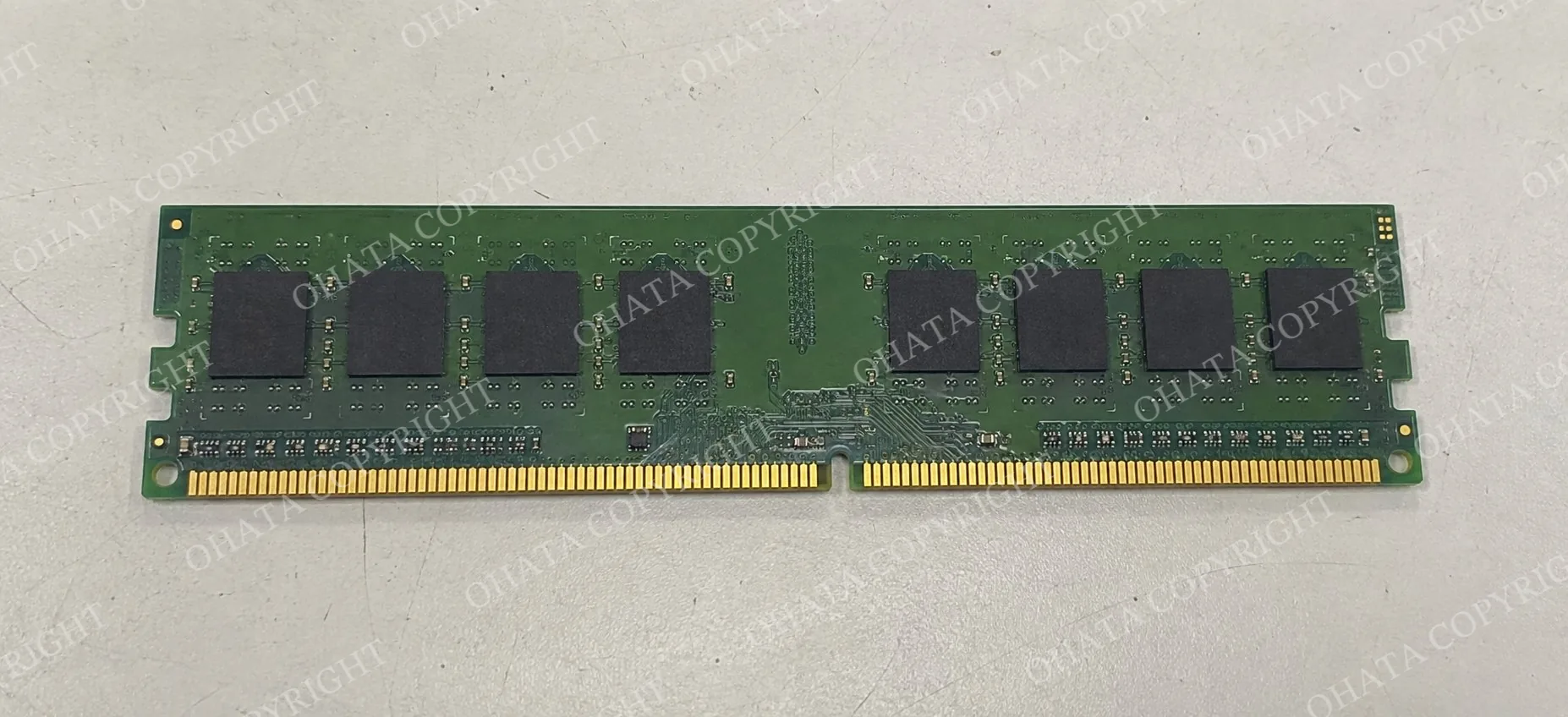
This guide explains how to identify gold fingers, why they are gold plated, how they differ from other gold-colored circuit board surfaces, and what they mean when electronic scrap is evaluated.
Why Are They Called Gold Fingers?
The name comes from their appearance. Each contact is long, narrow, and separated from the contacts beside it, creating a row that resembles fingers extending from the edge of a circuit board.
Gold fingers are designed to slide into a compatible slot. Spring contacts inside the slot press against them to create electrical connections between the inserted component and the main system.
Common identifying features include:
A position directly along an insertable board edge
Multiple narrow contacts arranged in a straight row
Even spacing between the individual contacts
A smooth, flat contact surface
One or more alignment notches
Contacts on one or both sides of the board
A gold-colored pad elsewhere on a circuit board is not necessarily a gold finger. The term specifically refers to repeated edge contacts designed to enter a slot connector.
Where Are Gold Fingers Found?
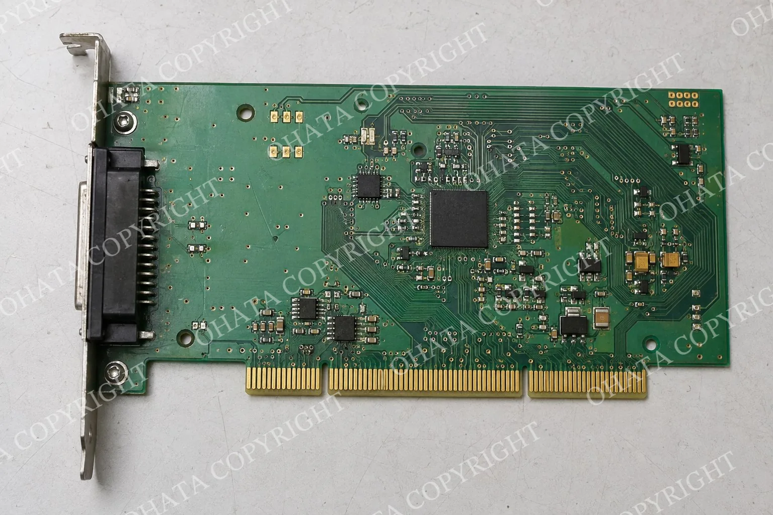
Gold fingers are commonly found on components that plug directly into another circuit board or system.
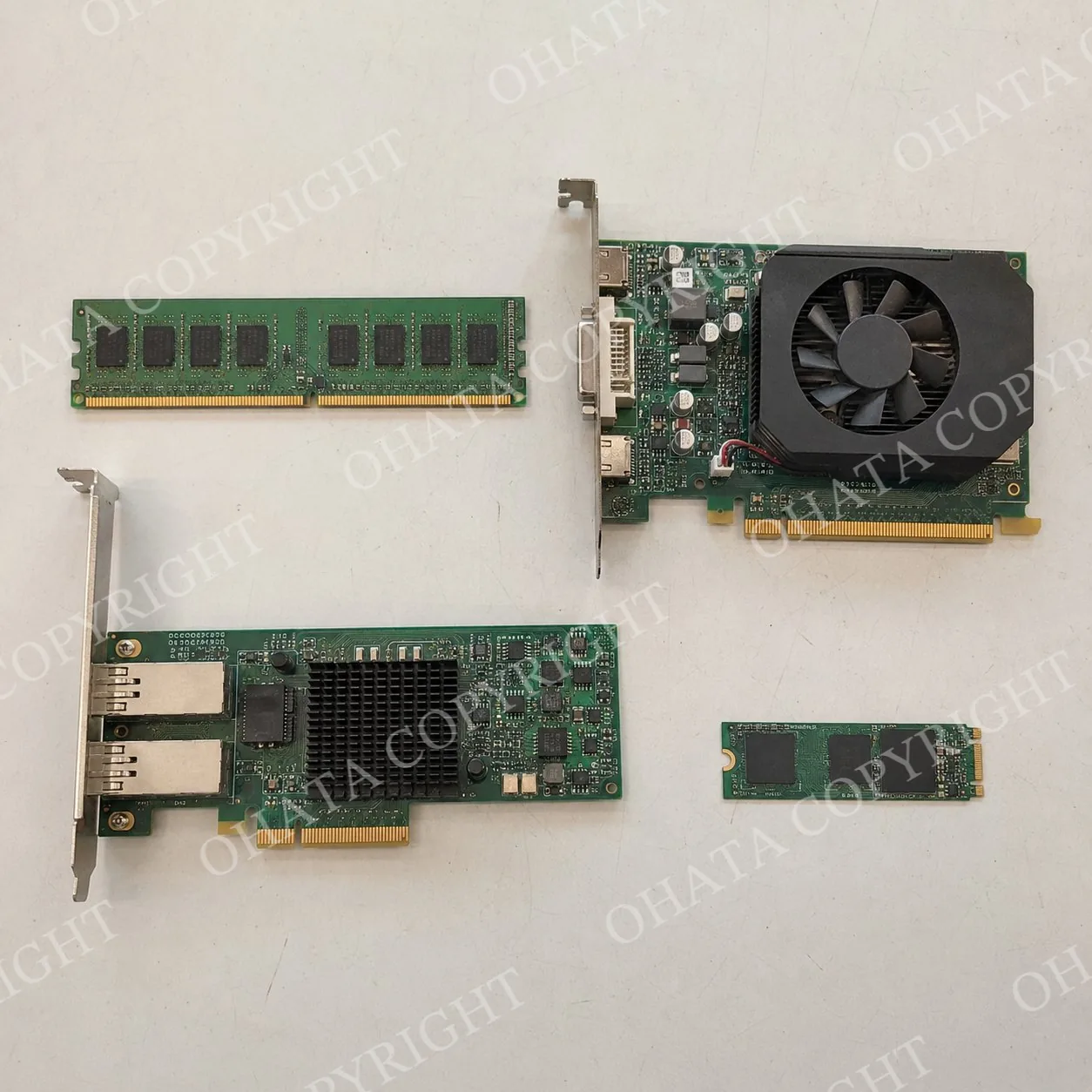
Examples include:
Desktop and laptop memory modules
Graphics cards
Network and sound cards
RAID and storage controller cards
PCI and PCI Express expansion cards
M.2 storage and wireless modules
Industrial control cards
Telecom and enterprise equipment boards
The number, length, spacing, and arrangement of the contacts depend on the component and connector standard.
What Is Beneath the Gold?
A typical gold finger has a copper contact beneath a nickel underlayer and an outer gold-plated surface. The exact materials and plating thickness depend on the component and manufacturing specification.
The typical structure is:
Copper: The copper contact connects to the electrical traces within the circuit board.
Nickel: The nickel acts as a barrier between the copper and gold and helps support the contact finish.
Gold plating: A thin outer layer provides a corrosion-resistant contact surface.
The nickel barrier helps limit the movement of copper into the gold layer. The gold visible from the outside is therefore only the surface of a layered electrical contact.
Why Is Gold Used on Electrical Contacts?
Copper conducts electricity well, but an exposed copper surface can oxidize. The resulting oxide layer can interfere with a dependable electrical connection.
Gold is useful on contact surfaces because it resists oxidation and corrosion. This helps maintain a stable electrical interface over time.
The effectiveness of the connection still depends on other factors, including:
Plating thickness
Surface cleanliness
Contact pressure
Wear
Connector design
Environmental conditions
Gold does not need to cover the entire circuit board. It is generally concentrated where a clean and reliable physical connection is especially important.
Gold Fingers Are Designed for Repeated Contact
Most exposed circuit board surfaces are not intended to experience repeated rubbing. Gold fingers are different.
Every time a card is inserted, spring contacts inside the slot slide across the plated surface. This movement helps establish the electrical connection, but it also creates friction and wear.
Gold fingers are designed around this repeated contact. Their plating finish, board-edge shape, surface condition, and the pressure of the connector all contribute to their reliability.
This is also why the finish used on gold fingers may differ from the gold-colored finish used on solderable circuit board pads.
Hard Gold vs. Immersion Gold
Not every gold-colored area on a circuit board has the same construction or purpose.
Hard Gold
Gold fingers commonly use an electrodeposited finish known as hard gold. This type of finish is formulated for greater wear resistance, often through the addition of a small amount of another metal.
Hard gold is suitable for surfaces that may experience repeated contact, such as:
Edge connectors
Keypad contacts
Test contacts
Other repeatedly contacted PCB surfaces
Immersion Gold
ENIG stands for electroless nickel immersion gold. It is a common circuit board surface finish used to protect exposed metal and provide a solderable surface.
ENIG may appear on solder pads, component mounting areas, and other exposed connection points. Its thin gold layer is not intended for the same repeated sliding-contact role as hard gold.
A gold finger and a gold-colored solder pad may look similar while having different finishes, thicknesses, and intended uses.
Why Is the Gold Applied Selectively?
Contact plating is normally limited to the area where the connector touches the board. This is known as selective plating.
Covering the entire circuit board with contact-grade gold would increase manufacturing costs without improving most of the board’s functions. Selective plating places the material where its corrosion resistance and contact performance are needed.
Because the plating is applied to a controlled area, the gold region often ends at a clean boundary. The exact appearance of this boundary varies according to the manufacturing process.
Why Is the Board Edge Sometimes Angled?
Many boards have a slightly beveled edge beside the gold fingers.
The bevel creates a gentler entry angle than a sharp, square board edge. It can help the board slide into its slot while reducing unnecessary stress on the plated contacts and the connector’s internal springs.
A properly formed bevel can also help reduce scraping during insertion.
What Do the Notches Do?
Notches within a row of gold fingers normally act as alignment keys. They help match a component with the correct type of slot.
Depending on the component, a notch can help prevent:
Installation in an incompatible connector
Insertion in the wrong orientation
Interchange between different component generations
Misalignment between the board and slot contacts
Different generations of memory, for example, may have notches in different positions even when the modules otherwise appear similar.
A clean, intentionally shaped notch is therefore part of the original design, not a missing or damaged contact area.
Why Are Some Fingers Shorter?
On some components, certain contacts are intentionally shorter than the surrounding fingers.
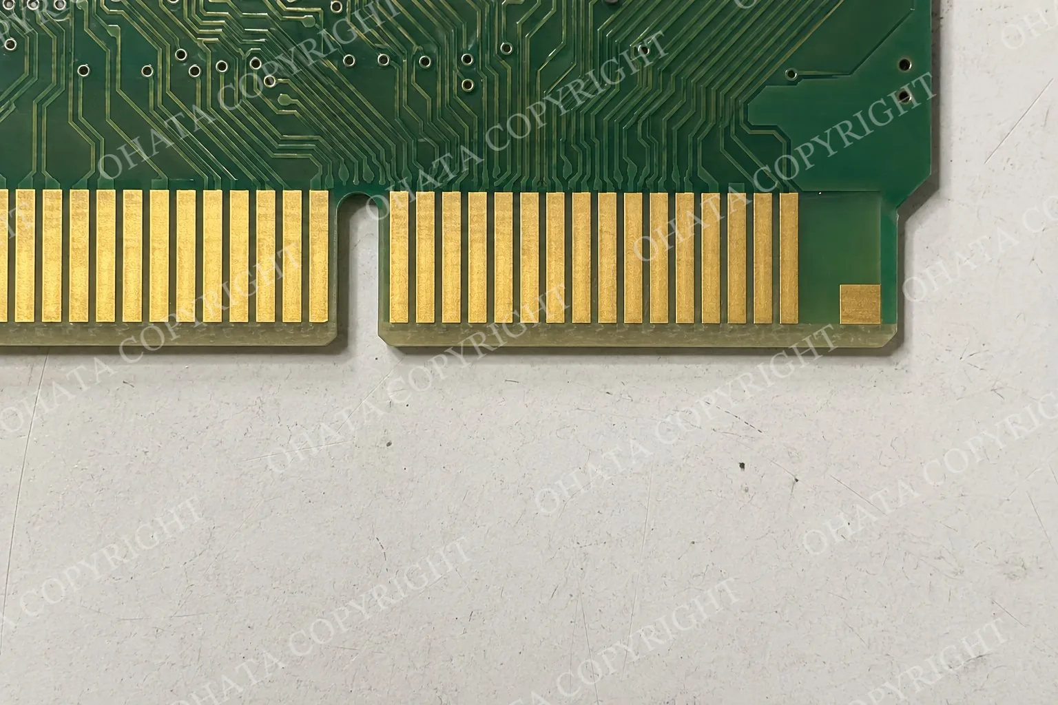
Deliberately staggered contact lengths allow some electrical connections to be made before others as the component enters the slot. Depending on the design, they may be used for grounding, power sequencing, presence detection, or controlled hot-plug operation.
Their exact purpose cannot be determined from length alone. A shorter finger is not necessarily worn or damaged when it has a clean, deliberate shape that matches the component’s design.
What Are the Straight Marks on Used Gold Fingers?
Light, straight marks are commonly caused by ordinary insertion and removal. They show where the slot’s spring contacts have rubbed against the plated surface.
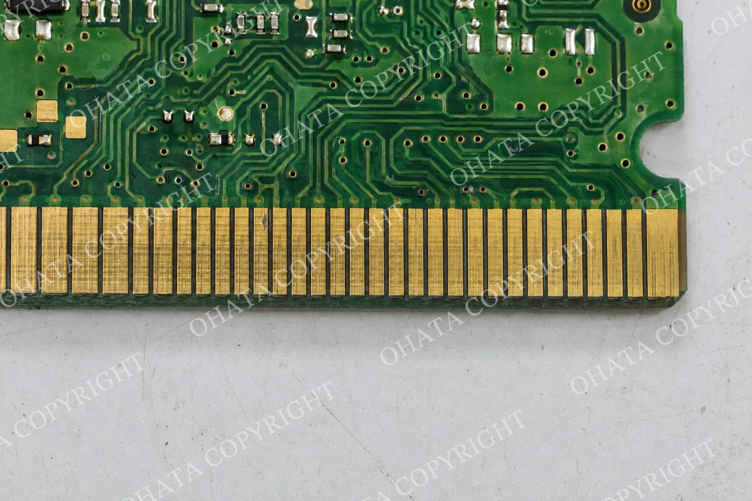
Normal insertion wear may appear as:
Fine parallel lines
Light polishing
Narrow contact tracks
Small differences in surface shine
Signs of more substantial damage may include:
Deep grooves
Missing or uneven plating
Silver-gray underlayers showing through
Reddish copper exposure
Burned or darkened areas
Corrosion
Cracks extending into the board
The presence of a few light lines does not automatically mean that a component is damaged. Their depth, severity, and extent are more important.
Can Gold Plating Be Identified by Color?
Color alone cannot reliably confirm that a surface is gold plated.
Brass, copper alloys, surface treatments, lighting, staining, and reflections can all create a yellow or gold-like appearance. Genuine gold plating can also vary in shade and brightness.
Visual inspection cannot reliably determine:
Whether a contact is genuinely gold plated
Which plating process was used
The thickness of the gold layer
The amount of recoverable gold
The complete recycling grade
The final buying value
A brighter or more yellow surface does not necessarily contain more gold.
Avoid scratching, filing, or chemically testing a component simply to inspect the metal beneath the surface. This can damage the item, affect its classification, and introduce unnecessary safety risks.
Should Gold Fingers Be Cut From Circuit Boards?
Gold fingers should not automatically be cut from complete memory modules or expansion cards.
A complete component preserves useful information about its original application, board construction, integrated circuits, component density, and overall condition. Removing the contact edge destroys some of that context.
Under electronic scrap purchasing standards, trimmed memory modules and expansion cards may be classified differently from qualifying complete components. Cutting off the gold fingers does not necessarily increase the material’s value and may result in a lower classification.
Unless a purchasing standard specifically requests separated material, keeping the component intact usually makes identification and evaluation easier.
Do Gold Fingers Determine Scrap Grade?
Gold fingers are an important identification feature, but they do not determine the grade or value of an entire component by themselves.
Memory modules, graphics cards, low-density peripheral cards, and industrial boards may all have gold fingers while belonging to different purchasing categories.
A complete evaluation may also consider:
Original item type
Board construction and component density
Completeness
Attached materials
Physical damage
Corrosion or contamination
Sorting quality
Under the Ohata classification system, each complete item is evaluated according to the applicable memory, circuit board, CPU, or electronic-component standard. There is no single universal grade for everything with gold fingers.
Ohata.ai Vision 1.0 may assist with preliminary identification from photographs. Final acceptance, classification, and buying price are determined after physical inspection and may depend on the material type, condition, completeness, quantity, and current buying standards.