

What Is a BGA Chip?
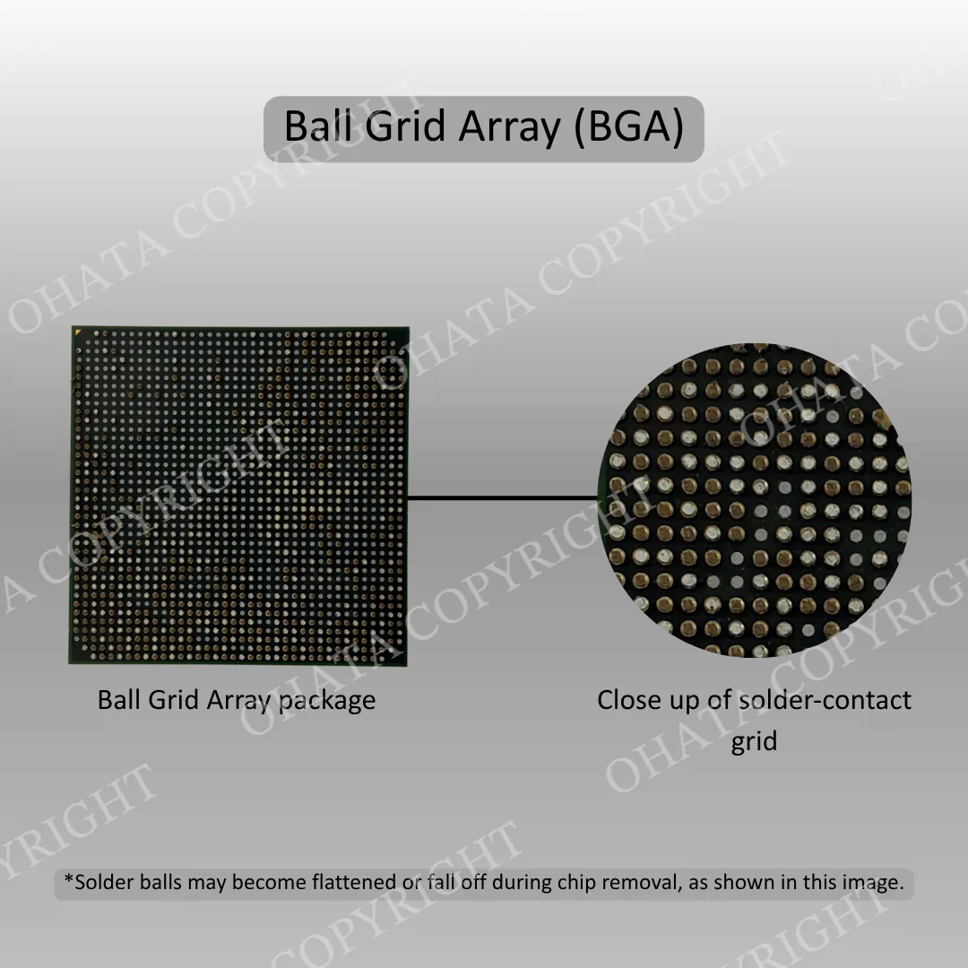
A BGA chip is an integrated circuit housed in a Ball Grid Array package. Instead of having long pins around its edges, it has an array of small solder balls on the underside. During circuit-board assembly, the balls align with matching pads and melt in a controlled reflow process. After cooling, the solder joints provide both electrical and mechanical connections between the package and the printed circuit board.
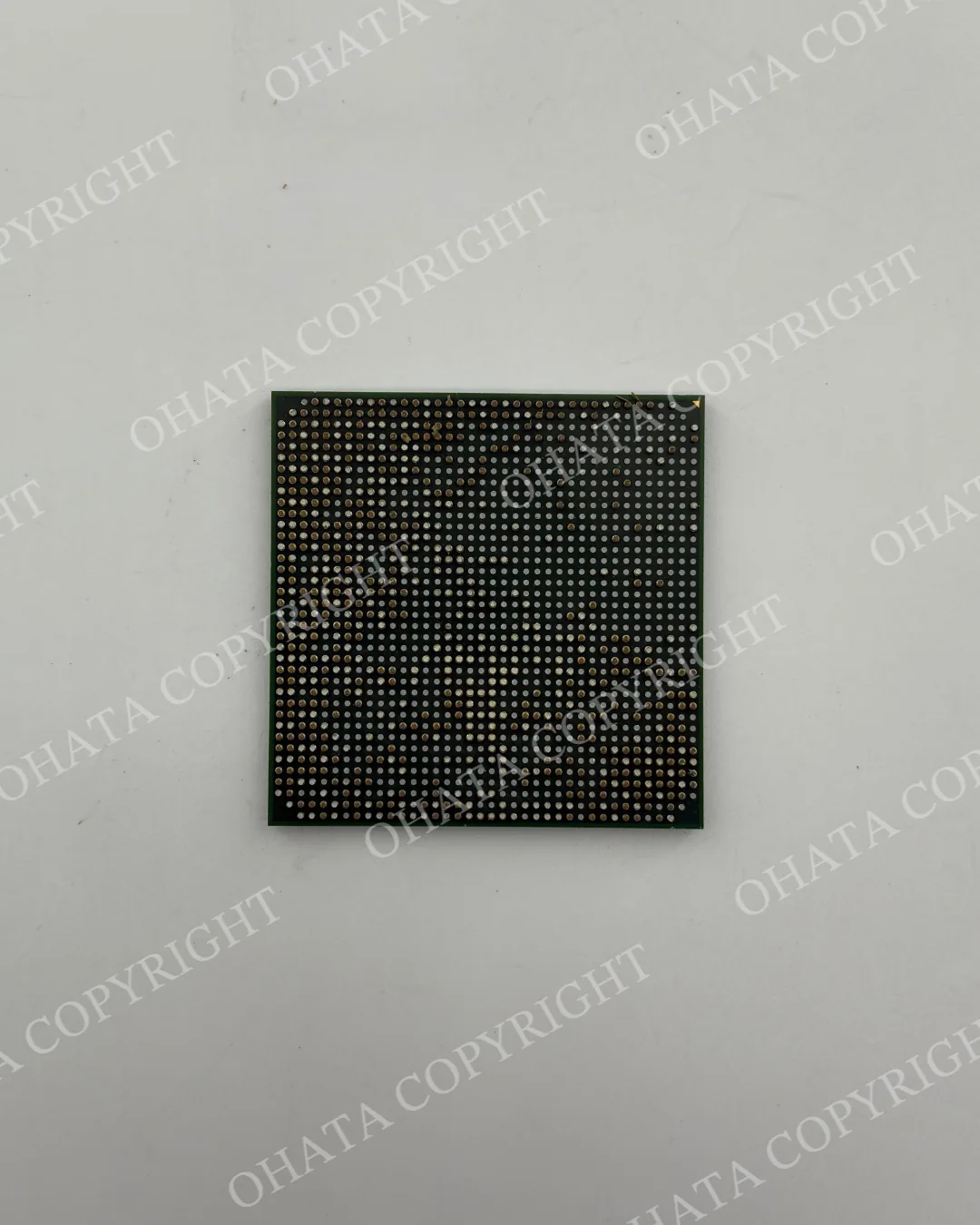
BGA describes how a chip is packaged and connected to a circuit board, not what the chip is designed to do. Many different components use BGA packaging, including laptop processors, graphics processors, chipsets, memory chips, FPGAs, and communications controllers. This means a square black chip is not automatically a CPU, and two BGA chips may serve completely different purposes. The package type alone does not determine the scrap grade; the device type, condition, markings, and other identifying features must be considered.
How BGA Packaging Works
Most BGA packages contain a silicon die, internal connections, a package substrate, protective material, and a grid of solder balls underneath. The die connects to the substrate through fine wire bonds or microscopic flip-chip bumps. Conductive paths inside the substrate then carry signals, power, and ground between the die and the solder balls. Depending on the package, the die may be covered by molding compound, a protective lid, or a heat spreader.
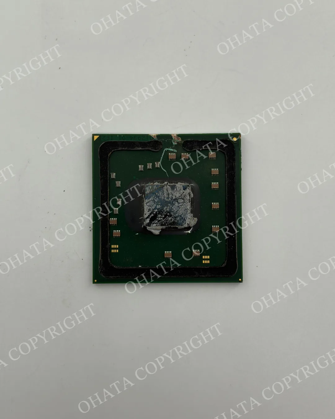
Because the connections are placed underneath the package, a BGA can fit many connections into a relatively small area. This design uses the entire underside of the package instead of limiting connections to its edges. It also shortens many of the electrical paths between the chip and the circuit board. During reflow soldering, the surface tension of the molten solder helps pull the package into alignment with the pads on the board.
Once a BGA is soldered in place, its solder joints are hidden from view. Manufacturers and repair specialists may use X-ray equipment, electrical testing, or boundary-scan testing to check for defects. Cracked or unreliable solder joints can result from thermal cycling, impact, board bending, poor reflow, contamination, or package warpage.
Common BGA package types include plastic BGA (PBGA), ceramic BGA (CBGA), fine-pitch BGA (FBGA), flip-chip BGA (FCBGA), and wafer-level BGA (WLBGA). Some devices also use package-on-package construction, in which compatible packages—such as a processor and memory—are stacked together. These names describe how a package is built or arranged; they do not determine what the device does or what scrap grade it receives.
Why Is BGA Packaging Used?
Manufacturers choose BGA packaging when a device needs many electrical connections in a compact area. Unlike leaded packages that place connections around the edges, a BGA uses much of the underside of the package. This allows more connections without making the chip unnecessarily large.
BGA packaging can also provide shorter electrical paths between the silicon die and the circuit board. Shorter paths can help reduce unwanted electrical resistance and interference, which is useful in processors, memory, graphics chips, networking devices, and other high-speed electronics.
Other advantages include:
More connections in less space
Compact circuit-board layouts
Better electrical performance at high speeds
Improved heat transfer through the package and circuit board
Self-alignment during reflow soldering as the molten solder helps center the package over its pads
BGA packaging also has tradeoffs. The solder joints are hidden beneath the package, making inspection and repair more difficult. Installing or removing a BGA normally requires controlled heating and specialized equipment. For devices that need to be easily replaced or upgraded, a socketed PGA or LGA package may be more practical.
The best package depends on the product’s design. BGA is commonly chosen for compact, high-performance electronics, while PGA, LGA, and leaded packages may be preferred when socket installation, easier inspection, or simpler assembly is more important.
Where Are BGA Chips Found?
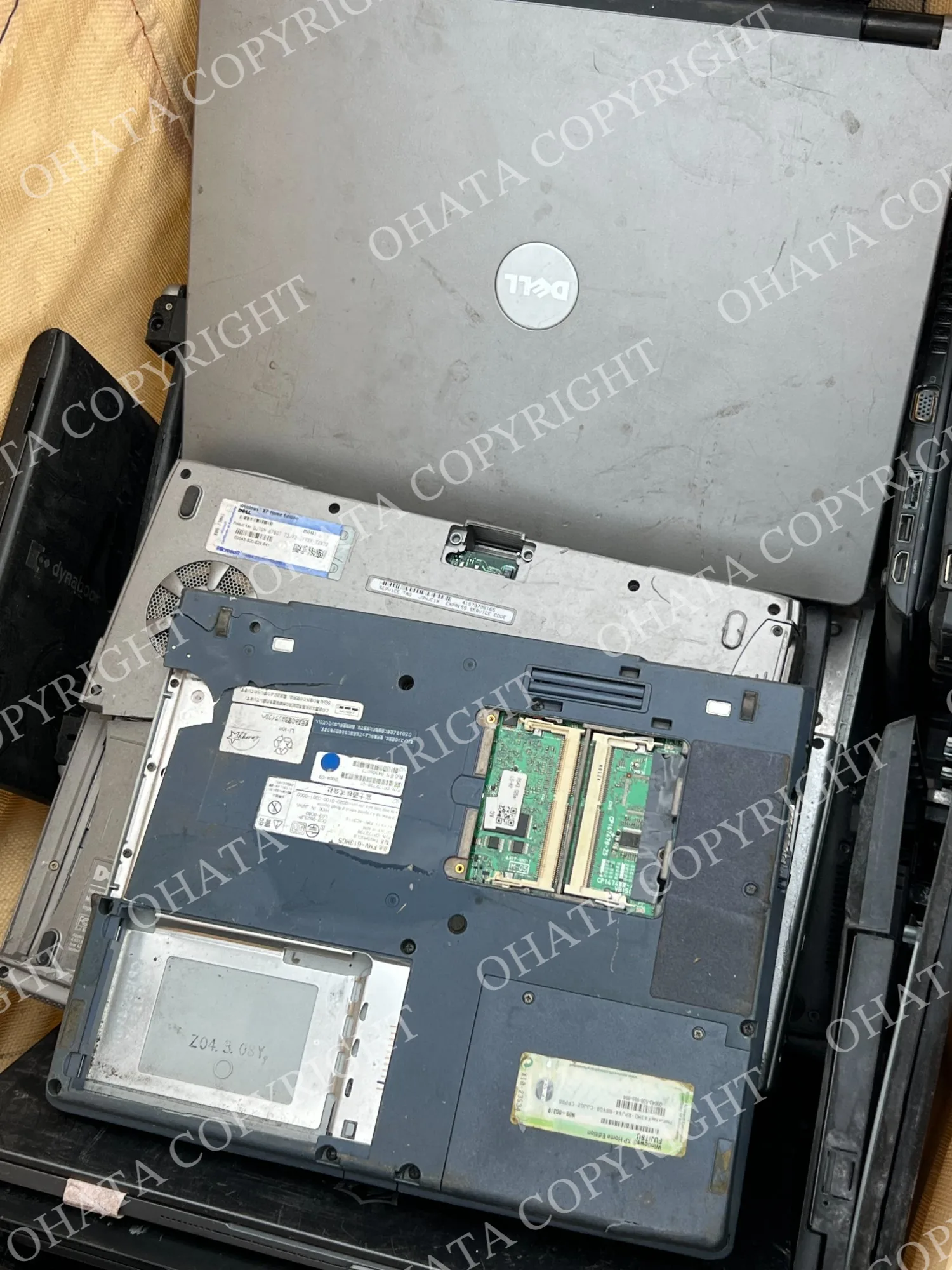
BGA devices are found in laptops, smartphones, graphics cards, game consoles, servers, networking equipment, storage devices, vehicles, industrial controllers, medical equipment, and telecommunications hardware. Large chips located beneath cooling assemblies may be CPUs or GPUs, while rows of smaller, matching chips are often memory. The size and location of a chip can provide useful clues, but checking its part number is the most reliable way to identify it.
When identifying a loose BGA device, inspect both the top and underside of the package. The underside should have a regular grid of solder balls or visible signs of the original solder-ball array. Record the manufacturer’s name, complete part number, package shape, ball pattern, and the equipment from which the chip was removed. Do not confuse a BGA package with an LGA package that has flat contact lands or a leaded IC with metal leads around its edges.
BGA Compared with PGA and LGA
Package | Connection style | Typical installation |
|---|---|---|
BGA | Solder balls beneath the package | Permanently soldered to the board |
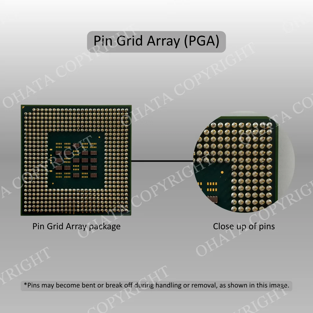
PGA | Projecting pins beneath the package | Inserted into a matching socket |
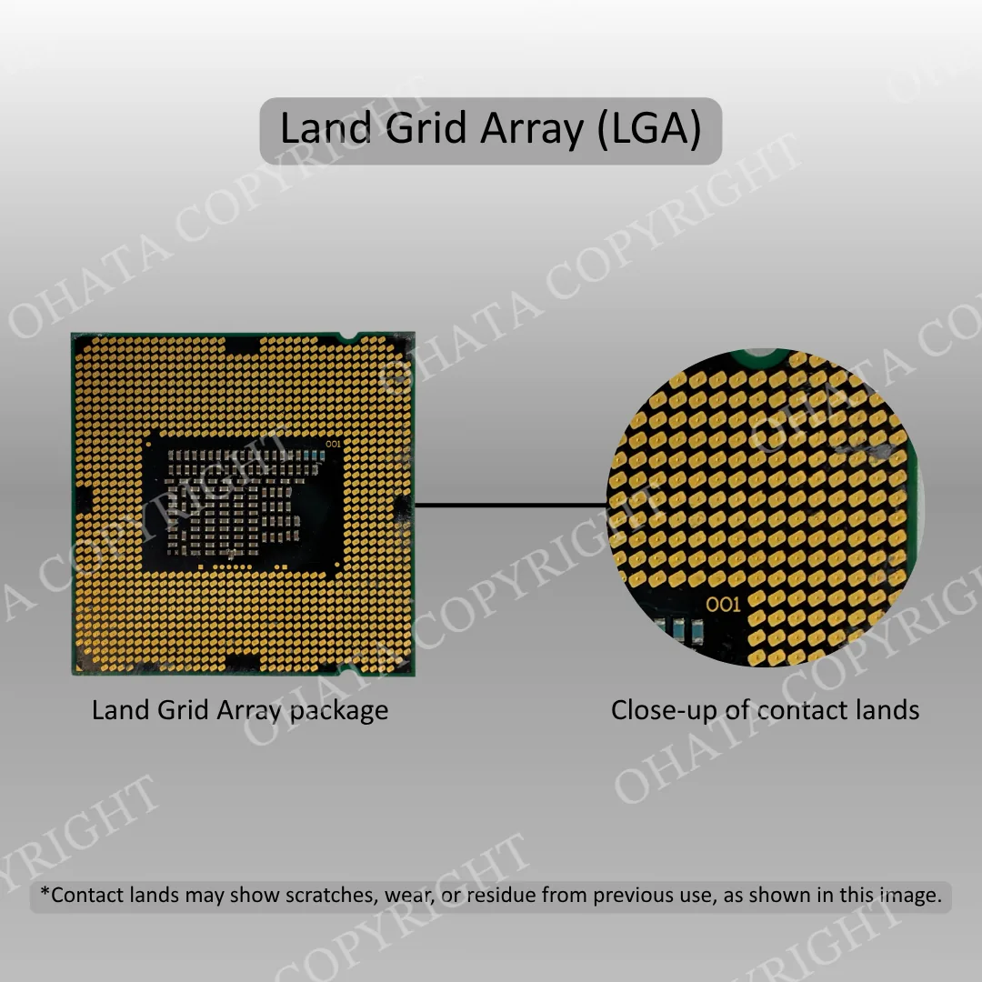
LGA | Flat contact lands beneath the package | Pressed against spring contacts in a socket |
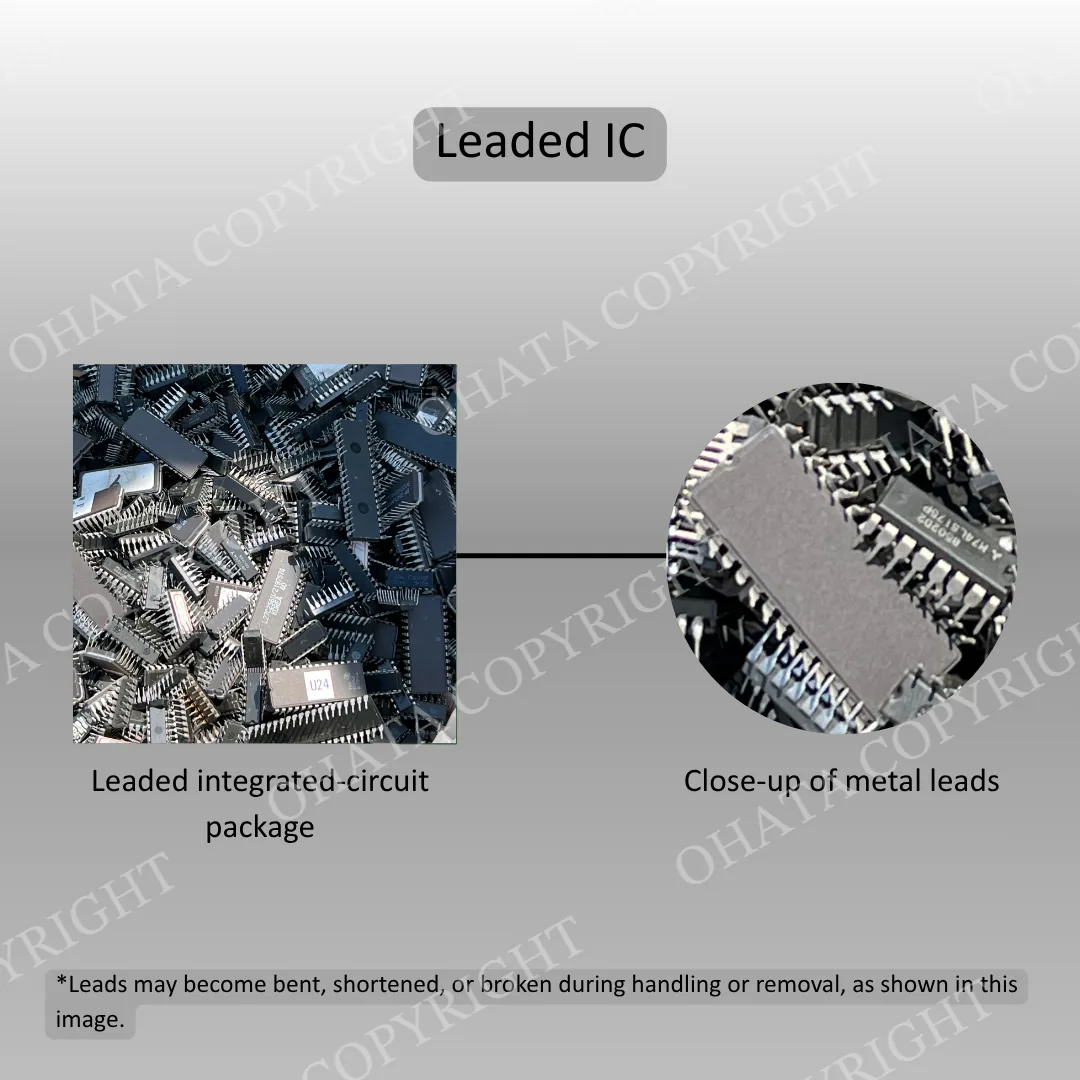
Leaded IC | Leads extend from the sides | Soldered through holes or onto surface pads |
BGA is often used when a device needs many connections in a compact space, but it is not always the best choice. Other packages may be selected when replaceability, easier inspection, simpler assembly, or lower manufacturing cost matters more.
PGA may be chosen when a device needs to be installed in a socket and replaced without soldering. Its pins are easy to inspect, and the processor can be removed with standard tools. However, PGA packages require more space than many BGA designs, and their exposed pins can bend or break.
LGA is often chosen for socketed desktop and server processors that may need to be replaced or upgraded. The processor has flat contact lands, while the delicate spring contacts remain inside the socket. This avoids placing fragile pins on the processor itself. Compared with BGA, LGA takes more board space and requires a socket and clamping mechanism.
A leaded package may be preferred when simpler assembly, visible solder joints, and easier inspection or repair are more important than fitting the highest number of connections into a small area. The leads can often be checked visually and soldered with less specialized equipment. Leaded packages are common for devices with modest connection counts, but they use more perimeter space and generally cannot provide the same connection density as BGA.
Why BGA May Still Be Preferred
BGA is usually the better option when the design calls for:
A high number of connections in a compact area
Short electrical paths for high-speed signals
Permanent attachment to the circuit board
Space-efficient product design
Automated high-volume assembly
The choice depends on the product’s needs. BGA favors compactness and connection density, PGA and LGA favor socketed replacement, and leaded packages favor visible connections and simpler inspection.
Buying, Downgrade, and Rejection Guidance
BGA material should be clean, dry, identifiable, and reasonably complete. Keep loose devices separate from circuit boards, batteries, heatsinks, fans, steel hardware, and packaging waste. When requesting an evaluation, provide clear photographs of the top markings and underside.
Material may be downgraded for:
Mixed or unidentified devices
Missing solder balls or removed dies
Cracked packages or damaged substrates
Corrosion, burned residue, or heavy thermal compound
Attached hardware or other contamination
Wet, chemically treated, hazardous, deliberately misrepresented, or heavily processed material may be rejected. Store loose devices in clean, dry, labeled containers, separating intact material from damaged or uncertain pieces.